Input Protection
PFI 0 and 3 are protected using diode clamps connected to positive and negative voltage supplies. PFI 0 and 3 are clamped to 5 V.
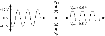
The following figure illustrates this circuit.

These diodes act as open circuits unless the I/O voltage levels go above Vp+ or below Vp-. When the I/O voltage exceeds Vp+/Vp-, the diodes become short circuits, clamping the input voltage to Vp+/Vp-. Therefore, these diodes prevent input voltages from going more than a diode drop, or approximately 0.5 V, beyond the positive or negative protection rails. The following diagram demonstrates the effect of the clamp.

DIO <0..15>, PFI <1..2>, DDC CLK OUT LVDS, DDC CLK OUT LVPECL, and STROBE are protected using robust pin electronics. Each channel is independently buffered using a robust pin electronic transceiver. These devices can protect against instantaneous shock and overvoltage cases.
In addition to the I/O circuit shown in the Channel Electronics diagram, data channels have a weak pull-up resistor (300 kΩ), internal to the I/0 buffer, to 3.3 V. This internal pull-up resistor is a fail-safe mechanism intended to set a known state when the receiver circuit is not being driven (tristate).
In a tristate condition, there is an equivalent RC circuit created from 3.3 V to ground. This RC equivalent is the interaction between these weak pull-up resistors and the capacitive transmission media (a cable or PCB, for example). As such, when the output terminals were previously tristated, some finite amount of time passes between the time when output terminals are driven to when the cable voltage reaches a steady common-mode value. This time varies with cable length and can take as many as several Sample clock periods.
 |
Note For this reason the NI 656x device does not support high-impedance initial and Idle states. Use the niHSDIO Tristate Channels VI or the niHSDIO_TristateChannels function. |
Refer to the NI 656x specifications for details on input protection.