Channel Electronics
The channel electronics of NI 654x devices consist of selectable voltage buffers, the appropriate termination resistors, and I/O protection diodes. Each I/O channel is capable of simultaneously driving and receiving data.
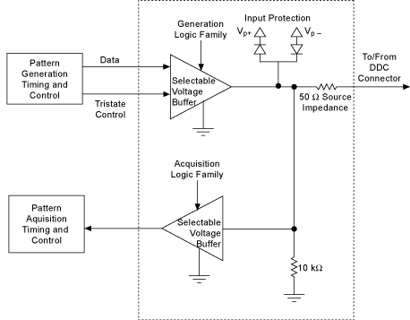
The following figure provides a basic block diagram for the channel electronics. Refer to NI 654x Block Diagram for a picture of how the channel electronics circuitry fits into the overall block diagram.
Dynamic Generation
For dynamic generation operations, the data appears at the input of the selectable voltage buffer after the Pattern Generation Timing and Control module gives the data the selected data position and data delay. The selectable voltage buffer converts the data signal to the user-selected logic family before sending the data signal to the DDC connector on the NI 654x front panel.
The selectable voltage buffer can be set to high-impedance generation with the Tristate Control line. The Tristate Control can be set automatically by the Initial and Idle States or can be set programmatically with the niHSDIO Tristate Channels VI or niHSDIO_TristateChannels function. When a channel is configured for open collector generation (supported for static generation only), the tristate control transforms logic 1's into Z states (high-impedance).
The protection diodes are critical for guarding against overvoltage situations. Refer to Input Protection for more information about this portion of the channel electronics.
Dynamic Acquisition
Patterns acquired by the NI 654x are received using a selectable voltage buffer. Refer to the NI 654x Specifications for the input voltage thresholds for each logic family setting.
The output of the selectable voltage buffer is sampled by the Pattern Acquisition Timing and Control module before being sent to the Pattern Acquisition Engine for storage into Acquisition Memory.
The input impedance is high impedance, referenced to ground.