Differential Logic Families
Differential logic families use differential voltage levels to measure the voltage difference between a pair of wires and interpret the difference as a binary one or zero.
Low-Voltage Differential Signaling (LVDS)
Low-voltage differential signaling (LVDS) is a low-noise, low-power, low-amplitude differential method for high-speed digital data transfer.
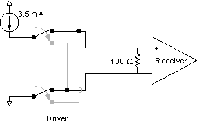
The following figure shows a diagram of a typical LVDS circuit.
A current source at the driver provides approximately 3.5 mA of current. The direction of the current depends on whether the driver drives a logic high level or low level. When the current reaches the receiver, a 100 Ω terminating resistor connects the two ends of the differential transmission line to provide a return path for the current. A voltage of approximately 350 mV (3.5 mA x 100 Ω) is established across the two input terminals of the receiver. The differential voltage at the receiver is either positive or negative, depending on the direction of the current. The receiver recognizes a positive differential voltage signal as a logic high level (binary 1) and a negative differential voltage as a logic low level (binary 0).
The electrical characteristics of an LVDS signal offers many performance improvements compared to single-ended standards. For example, since the received voltage is a differential between two signals, the voltage swing between the logic high level and low level state can be smaller, allowing for faster rise and fall times and thus faster toggle and data rates. Also, as with LVPECL circuits, the differential receiver is less susceptible to common-mode noise than single-ended transmission methods.
The LVDS standard defines the electrical aspects of this type of data transmission. The standard defines driver and receiver electrical characteristics only. The standard does not create protocol, interconnect, or connector definitions because these aspects are application-specific.
For more information on LVDS, refer to the Understanding LVDS for Digital Test Systems application note on ni.com.
 |
Note Refer to the ANSI/TIA/EIA-644-A electrical characteristics standard, Electrical Characteristics of Low-Voltage Differential Signaling (LVDS) Interface Circuits, Revision A, 2001 edition for more information about the LVDS standard. |
Low-Voltage Positive Emitter-Coupled Logic (LVPECL)
Emitter-Coupled Logic circuits use a design with transistors that steer current through gates to compute logical functions. Because the transistors are always in the active region, they can change state very rapidly, so ECL circuits can operate at very high speeds.
LVPECL circuits are a type of ECL circuit that require a pair of signal lines for each channel. The differential transmission scheme is less susceptible to common-mode noise than single-ended transmission methods. LVPECL circuits are designed for use with supply voltages of 3 V or 3.3 V.