Block Diagram
The following figure is a block diagram illustrating the main functional units and data flow of the NI 655x. The text that follows the figure describes the basic elements of the diagram and provides links to sections with more detailed information about some of the blocks.
Click hotspots within the graphic for more detailed information about that functional block.
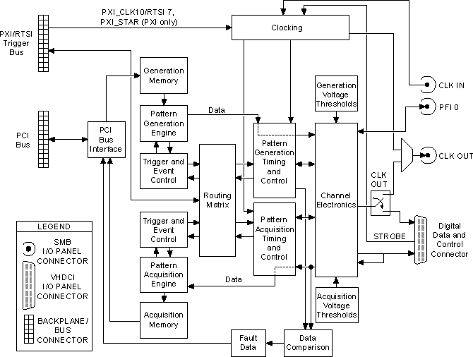
The Clocking module selects and distributes the clocks for the dynamic generation and dynamic acquisition operations.
For dynamic generation operations, the user-supplied data is loaded from the host computer memory into the onboard Generation Memory. The Pattern Generation Engine retrieves data from Generation Memory and executes the script functionality while interacting with the associated Trigger and Event control module. The Pattern Generation Engine then sends the data to the Pattern Generation Timing and Control module, where the data is given the selected data position and data delay and is then sent to the Channel Electronics drivers. The Channel Electronics drivers generate the data at the user-defined voltage levels.
For dynamic acquisition operations, signals arrive at the Channel Electronics comparators, where the signal levels are compared to the user-defined voltage thresholds. The Timing and Control module samples the data using the selected clock, data position, and data delay values and passes the data to the Pattern Acquisition Engine. The Pattern Acquisition Engine and the Trigger and Event Control module recognize triggers and determine when the data should be stored into Acquisition Memory. The acquired data can then be fetched by the host computer.