NI PXI-2532 2-Wire 16×16 Matrix Topology
The NI TB-2645 terminal block creates a 2-wire 16×16 matrix topology with the NI PXI-2532. The following figure represents the NI PXI-2532 in the 2-wire 16×16 matrix topology.
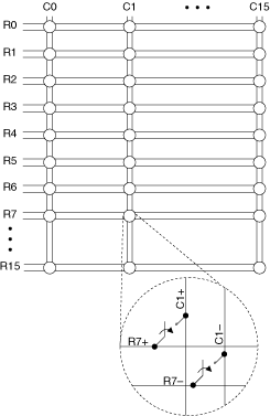
Making a Connection
Both the scanning command, r6->c1;, and the immediate operation, niSwitch Connect Channels VI or the niSwitch_Connect function with parameters r6 and c1, result in the following connections:
signal connected to R6+ is routed to C1+
signal connected to R6– is routed to C1–
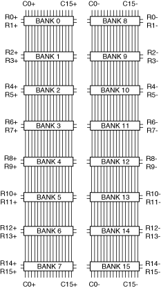
Terminal Block Connections
The NI TB-2645 terminal block connects the banks of the NI PXI-2532 to create the 2-wire 16×16 matrix topology. The following figure illustrates how the native banks on the NI PXI-2532 connect using the NI TB-2645 to create the 2-wire 16×16 matrix topology.
Bank Connection Diagram
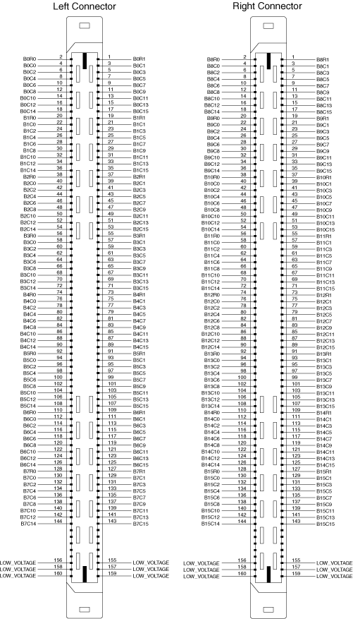
The following tables list the pin assignments for the NI TB-2645 column connection board.
Column Connection Board Column Pin Assignment
| Pin Number | Column | Pin Number | Column | Pin Number | Column | Pin Number | Column |
|---|---|---|---|---|---|---|---|
| J3 Pin 1 | C0+ | J3 Pin 9 | C4+ | J3 Pin 17 | C8+ | J3 Pin 25 | C12+ |
| J3 Pin 2 | C0– | J3 Pin 10 | C4– | J3 Pin 18 | C8– | J3 Pin 26 | C12– |
| J3 Pin 3 | C1+ | J3 Pin 11 | C5+ | J3 Pin 19 | C9+ | J3 Pin 27 | C13+ |
| J3 Pin 4 | C1– | J3 Pin 12 | C5– | J3 Pin 20 | C9– | J3 Pin 28 | C13– |
| J3 Pin 5 | C2+ | J3 Pin 13 | C6+ | J3 Pin 21 | C10+ | J3 Pin 29 | C14+ |
| J3 Pin 6 | C2– | J3 Pin 14 | C6– | J3 Pin 22 | C10– | J3 Pin 30 | C14– |
| J3 Pin 7 | C3+ | J3 Pin 15 | C7+ | J3 Pin 23 | C11+ | J3 Pin 31 | C15+ |
| J3 Pin 8 | C3– | J3 Pin 16 | C7– | J3 Pin 24 | C11– | J3 Pin 32 | C15– |
 |
Note The column connection board J2 connector is not used in this configuration. |
Row Pin Connections
The following tables list the pin assignments for row connection.
| Pin Number | Row |
|---|---|
| J2 Pin 1 | R0+ |
| J2 Pin 2 | R0– |
| J2 Pin 3 | R1+ |
| J2 Pin 4 | R1– |
| J2 Pin 5 | R2+ |
| J2 Pin 6 | R2– |
| J2 Pin 7 | R3+ |
| J2 Pin 8 | R3– |
| J2 Pin 9 | R4+ |
| J2 Pin 10 | R4– |
| J2 Pin 11 | R5+ |
| J2 Pin 12 | R5– |
| J2 Pin 13 | R6+ |
| J2 Pin 14 | R6– |
| J2 Pin 15 | R7+ |
| J2 Pin 16 | R7– |
| Pin Number | Row |
|---|---|
| J3 Pin 1 | R8+ |
| J3 Pin 2 | R8– |
| J3 Pin 3 | R9+ |
| J3 Pin 4 | R9– |
| J3 Pin 5 | R10+ |
| J3 Pin 6 | R10– |
| J3 Pin 7 | R11+ |
| J3 Pin 8 | R11– |
| J3 Pin 9 | R12+ |
| J3 Pin 10 | R12– |
| J3 Pin 11 | R13+ |
| J3 Pin 12 | R13– |
| J3 Pin 13 | R14+ |
| J3 Pin 14 | R14– |
| J3 Pin 15 | R15+ |
| J3 Pin 16 | R15– |
Pinout
The following figure identifies the pins for the NI PXI-2532.
 |
Caution Low-voltage pins are reserved for future use. These pins should remain disconnected and isolated from row and column channels when high voltage is present. |