NI PXI-2532 1-Wire 4×128 Matrix Topology
The NI TB-2640 terminal block creates a 1-wire 4×128 matrix topology with the NI PXI-2532. The following figure represents the NI PXI-2532 in the 1-wire 4×128 matrix topology.
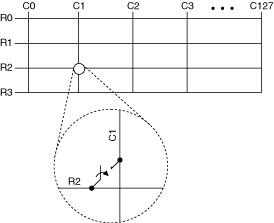
Making a Connection
Both the scanning command, r2->c1;, and the immediate operation, niSwitch Connect Channels VI or the niSwitch_Connect function with parameters r2 and c1, result in the following connection:
signal connected to R2 is routed to C1
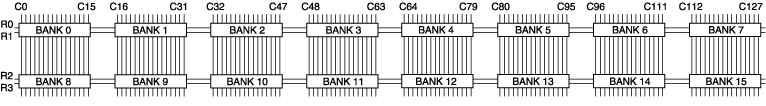
Terminal Block Connections
The NI TB-2640 terminal block connects banks of the NI PXI-2532 to create the 1-wire 4×128 matrix topology. The following figure illustrates how the native banks of the NI PXI-2532 connect using the NI TB-2640 to create the 1-wire 4×128 matrix topology.
Bank Connection Diagram
The following tables list the pin assignments for the NI TB-2640 upper and lower column connection boards.
Upper Column Connection Board Column Pin Assignment
| Pin Number | Column | Pin Number | Column | Pin Number | Column | Pin Number | Column |
|---|---|---|---|---|---|---|---|
| J3 Pin 1 | C127 | J3 Pin 9 | C119 | J3 Pin 17 | C111 | J3 Pin 25 | C103 |
| J3 Pin 2 | C126 | J3 Pin 10 | C118 | J3 Pin 18 | C110 | J3 Pin 26 | C102 |
| J3 Pin 3 | C125 | J3 Pin 11 | C117 | J3 Pin 19 | C109 | J3 Pin 27 | C101 |
| J3 Pin 4 | C124 | J3 Pin 12 | C116 | J3 Pin 20 | C108 | J3 Pin 28 | C100 |
| J3 Pin 5 | C123 | J3 Pin 13 | C115 | J3 Pin 21 | C107 | J3 Pin 29 | C99 |
| J3 Pin 6 | C122 | J3 Pin 14 | C114 | J3 Pin 22 | C106 | J3 Pin 30 | C98 |
| J3 Pin 7 | C121 | J3 Pin 15 | C113 | J3 Pin 23 | C105 | J3 Pin 31 | C97 |
| J3 Pin 8 | C120 | J3 Pin 16 | C112 | J3 Pin 24 | C104 | J3 Pin 32 | C96 |
| Pin Number | Column | Pin Number | Column | Pin Number | Column | Pin Number | Column |
|---|---|---|---|---|---|---|---|
| J2 Pin 1 | C95 | J2 Pin 9 | C87 | J2 Pin 17 | C79 | J2 Pin 25 | C71 |
| J2 Pin 2 | C94 | J2 Pin 10 | C86 | J2 Pin 18 | C78 | J2 Pin 26 | C70 |
| J2 Pin 3 | C93 | J2 Pin 11 | C85 | J2 Pin 19 | C77 | J2 Pin 27 | C69 |
| J2 Pin 4 | C92 | J2 Pin 12 | C84 | J2 Pin 20 | C76 | J2 Pin 28 | C68 |
| J2 Pin 5 | C91 | J2 Pin 13 | C83 | J2 Pin 21 | C75 | J2 Pin 29 | C67 |
| J2 Pin 6 | C90 | J2 Pin 14 | C82 | J2 Pin 22 | C74 | J2 Pin 30 | C66 |
| J2 Pin 7 | C89 | J2 Pin 15 | C81 | J2 Pin 23 | C73 | J2 Pin 31 | C65 |
| J2 Pin 8 | C88 | J2 Pin 16 | C80 | J2 Pin 24 | C72 | J2 Pin 32 | C64 |
Lower Column Connection Board Column Pin Assignment
| Pin Number | Column | Pin Number | Column | Pin Number | Column | Pin Number | Column |
|---|---|---|---|---|---|---|---|
| J3 Pin 1 | C0 | J3 Pin 9 | C8 | J3 Pin 17 | C16 | J3 Pin 25 | C24 |
| J3 Pin 2 | C1 | J3 Pin 10 | C9 | J3 Pin 18 | C17 | J3 Pin 26 | C25 |
| J3 Pin 3 | C2 | J3 Pin 11 | C10 | J3 Pin 19 | C18 | J3 Pin 27 | C26 |
| J3 Pin 4 | C3 | J3 Pin 12 | C11 | J3 Pin 20 | C19 | J3 Pin 28 | C27 |
| J3 Pin 5 | C4 | J3 Pin 13 | C12 | J3 Pin 21 | C20 | J3 Pin 29 | C28 |
| J3 Pin 6 | C5 | J3 Pin 14 | C13 | J3 Pin 22 | C21 | J3 Pin 30 | C29 |
| J3 Pin 7 | C6 | J3 Pin 15 | C14 | J3 Pin 23 | C22 | J3 Pin 31 | C30 |
| J3 Pin 8 | C7 | J3 Pin 16 | C15 | J3 Pin 24 | C23 | J3 Pin 32 | C31 |
| Pin Number | Column | Pin Number | Column | Pin Number | Column | Pin Number | Column |
|---|---|---|---|---|---|---|---|
| J2 Pin 1 | C32 | J2 Pin 9 | C40 | J2 Pin 17 | C48 | J2 Pin 25 | C56 |
| J2 Pin 2 | C33 | J2 Pin 10 | C41 | J2 Pin 18 | C49 | J2 Pin 26 | C57 |
| J2 Pin 3 | C34 | J2 Pin 11 | C42 | J2 Pin 19 | C50 | J2 Pin 27 | C58 |
| J2 Pin 4 | C35 | J2 Pin 12 | C43 | J2 Pin 20 | C51 | J2 Pin 28 | C59 |
| J2 Pin 5 | C36 | J2 Pin 13 | C44 | J2 Pin 21 | C52 | J2 Pin 29 | C60 |
| J2 Pin 6 | C37 | J2 Pin 14 | C45 | J2 Pin 22 | C53 | J2 Pin 30 | C61 |
| J2 Pin 7 | C38 | J2 Pin 15 | C46 | J2 Pin 23 | C54 | J2 Pin 31 | C62 |
| J2 Pin 8 | C39 | J2 Pin 16 | C47 | J2 Pin 24 | C55 | J2 Pin 32 | C63 |
Row Pin Connections
The NI TB-2640 provides two ribbon cable headers for row connection. Use one cable header to connect to your application. Use the other cable header for column expansion.
The following table lists the pin assignments for row connection.
| Pin Number | Row |
|---|---|
| 1 | RO |
| 2 | R1 |
| 3 | R2 |
| 4 | R3 |
| 5–16 | — |
Row Protection Bypass Header
The row ribbon cable headers are isolated from the reed relays through 100 Ω resistors. To bypass these resistors, install a jumper in the appropriate position of J5 on the switch module interface board. The following table lists possible jumper locations.
| Pin Connected | Bypassed Row |
|---|---|
| 1–2 | R0 |
| 5–6 | R1 |
| 9–10 | R2 |
| 13–14 | R3 |
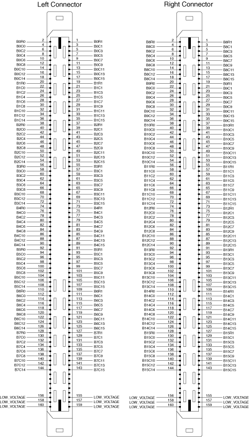
Pinout
The following figure identifies the pins for the NI PXI-2532.
 |
Caution Low-voltage pins are reserved for future use. These pins should remain disconnected and isolated from row and column channels when high voltage is present. |