NI 5401/5411/5431 Phase-Locked Loops and Module Synchronization
From NI Signal Generator
NI 5401/5411/5431
Phase-Locked Loops and Module Synchronization
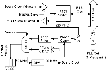
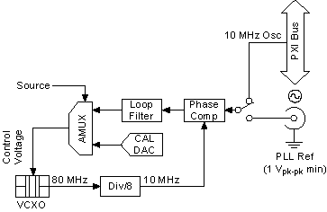
The PLL consists of a voltage-controlled crystal oscillator (VCXO) with a tuning range of ±100 ppm. This VCXO generates the main clock of 80 MHz.
The PLL can lock to a Reference clock source from the external connector, from a RTSI Osc line on the RTSI bus for NI PCI signal generators, or from a 10 MHz Osc line on the PXI backplane bus for NI PXI signal generators. You can also tune the PLL internally using a calibration DAC (CalDAC). NI performs this tuning during manufacturing.
The reference and VCXO clock are compared by a phase comparator running at 1 MHz. The loop filters the error signal and sends it to the control pin of the VCXO to complete the loop.
The following figure shows the block diagram for the NI signal generators PCI devices PLL circuit.
The following figure shows the block diagram for NI signal generators PXI devices PLL circuit.
You can frequency lock to an external Reference clock source of 1 MHz and from 5 MHz to 20 MHz in 1 MHz increments. The PLL can lock to a signal level of at least 1 Vpk-pk.
| Caution Do not increase the voltage level of the clock signal at the PLL reference input connector by more than the specified limit, 5 Vpk-pk. |
| Notes If two or more NI 5401 signal generators are locked to each other using the same Reference clock, they are frequency locked, but the phase relationship is indeterminate. | |
| When generating a video waveform, do not phase lock the NI 5431 if the attribute or property for Video Waveform Type is used to set the internal frequency of the device. |
The VCXO output of 80 MHz is further divided by four to send a 20 MHz device clock signal to the RTSI bus.