NI 5421/5422/5441/5442
Low-Voltage Differential Signaling (LVDS)
Low-voltage differential signaling (LVDS) is a low-noise, low-power, low-amplitude method for high-speed digital data transfer.
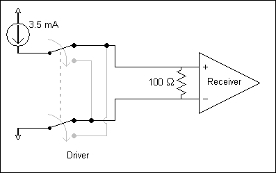
The following figure shows a diagram of a typical LVDS circuit.

As you can see in the previous figure, a current source at the driver provides approximately 3.5 mA of current. The direction of the current across the transmission line depends on whether the driver drives a logic high level or low level. When the current reaches the receiver, a 100 Ω terminating resistor connects the two ends of the differential transmission line to provide a return path for the current. In addition, a voltage of approximately 350 mV is established across the two input terminals of the receiver. The differential voltage at the receiver is either positive or negative, depending on the direction of the current. The receiver recognizes a positive voltage signal as a logic high level (1) and a negative voltage as a logic low level (0).
The electrical characteristics of an LVDS signal offers some performance improvements compared to single-ended standards. For example, since the received voltage is a differential between two signals, the voltage difference between the logic high level and low level state can be smaller, allowing for faster rise and fall times. Also, the differential transmission scheme is less susceptible to common-mode noise than single-ended transmission methods.
The LVDS standard defines the electrical aspects of this type of data transmission. The standard defines driver and receiver characteristics only. However, the standard does not create protocol, interconnect, or connector definitions because these aspects are application specific.
 |
Note Refer to the ANSI/TIA/EIA-644-A electrical characteristics standard, Electrical Characteristics of Low-Voltage Differential Signaling (LVDS) Interface Circuits, Revision A, 2001 edition for more information. |