NI 5402/5406 Exporting Clocks
From NI Signal Generator
NI 5402/5406
Exporting Clocks
The NI 5402/5406 provides two resources for exporting your clocks and multiple destinations to route to.
The following table shows the available clock signals that can be routed to devices external to the NI 5402/5406 and the destination options.
| Clock to be Exported | Destination Options |
|---|---|
Sample Clock |
SYNC OUT/PFI 0 and PFI 1 BNC connector |
PXI_Trig<0..6> (PXI), RTSI<0..6> (PCI) |
|
Reference Clock |
SYNC OUT/PFI 0 and PFI 1 BNC connector |
PXI_Trig<0..6> (PXI), RTSI<0..6> (PCI) |
|
Onboard Reference Clock |
RTSI7 |
Sample Clock
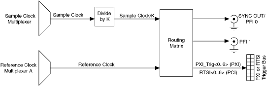
For synchronization purposes, the NI 5402/5406 allows you to export your Sample clock so that other devices can have the same timing as the NI 5402/5406. The Sample clock can be routed to the SYNC OUT/PFI 0 and PFI 1 front panel BNC connectors, PXI_Trig<0..6> lines on the PXI trigger bus, or the RTSI<0..6> (PCI) lines.
Additionally, the exported clock can be divided down by an integer value (no less than 2) before being exported to the SYNC OUT/PFI 0 and PFI 1 BNC connectors, PXI_Trig<0..6> lines, or the RTSI<0..6> (PCI) lines. Refer to the Exported Sample Clock Divisor property or the NIFGEN_ATTR_EXPORTED_SAMPLE_CLOCK_DIVISOR attribute for more information about configuring the Sample clock divisor.
| Note For the maximum frequency that can be routed to the PXI trigger bus, or the RTSI<0..6> (PCI) lines, refer to the module specifications. |
Reference Clock
For synchronization purposes, the NI 5402/5406 allows you to export your PLL Reference clock so that other devices can lock their clock sources to the same signal. Referring to the previous image, this clock is the actual clock that is configured for the NI 5402/5406 phase-locked loop circuit to use as a reference. You must have a Reference clock configured as a PLL Reference clock source for the signal to be available for exporting. The Reference clock can be routed to the SYNC OUT/PFI 0 and PFI 1 BNC connectors on the front panel, the PXI_Trig<0..6> lines on the PXI trigger bus, or the RTSI<0..6> (PCI) lines.
| Note Although NI-FGEN allows values for Reference clock frequency on the NI 5402/5406 from 1 MHz to 20 MHz in 1 MHz increments, the NI 5402/5406 specifications are only valid with Reference clock frequencies from 5 MHz to 20 MHz. |
Onboard Reference Clock
The onboard Reference clock is a dedicated 10 MHz clock for PCI modules only. The onboard Reference clock can only be exported to RTSI7, for other modules to use, and to reimport as the Reference clock. You can export the onboard Reference clock to other modules on RTSI7 and then reimport it so that all devices (including the master) can use the same Reference clock.
Destination Options
SYNC OUT/PFI 0 and PFI 1–The Sample clock and the Reference clock can be exported to the SYNC OUT/PFI 0 and PFI 1 BNC connectors on the front panel to synchronize external devices. You must configure the device to export the desired clock to the PFI BNC connectors.
| Notes NI-FGEN routes SYNC OUT to the SYNC OUT/PFI 0 connector by default. To use the SYNC OUT/PFI 0 to import or export any other signal, you must unroute SYNC OUT by using the niFgen Export Signal VI or the niFgen_ExportSignal function. If you route a signal to SYNC OUT/PFI 0 without first unrouting SYNC OUT, NI-FGEN returns error -89137 (Hex 0xBFFA6B8E) noting that the specified route could not be satisfied. | |
| SYNC OUT/PFI 0 driver circuitry has been optimized to have lower jitter than PFI 1 for exporting the SYNC OUT Sample clock or the PLL Reference clock source. |
PXI_Trig<0..6>–The Sample clock and the Reference clock can be exported to the PXI_Trig lines or RTSI (PCI) lines. The PXI/PCI standard allows for devices to route signals to other devices in your PXI chassis to enhance device to device synchronization. Refer to the chassis documentation for specifications to ensure the reference signal is within tolerance. You must configure the device to export the desired clock to the PXI_Trig line or RTSI line. When exporting signals, PXI_Trig<0..6> is equivalent to RTSI_<0..6>
Refer to the niFgen Export Signal VI or the niFgen_ExportSignal function for more information about configuring the destinations for the desired clock signal.