NI 5411/5431 Digital Pattern Generation
From NI Signal Generator
NI 5411/5431
Digital Pattern Generation
The NI 5411/5431 has 16-bit digital pattern generation outputs at the digital connector. This digital data is first synchronized to the Sample clock and then buffered and sent to the connector through a 68 Ω series resistor. The Sample clock is also buffered and sent to the digital connector to latch the data externally. The following figure shows the data path for digital pattern generation.
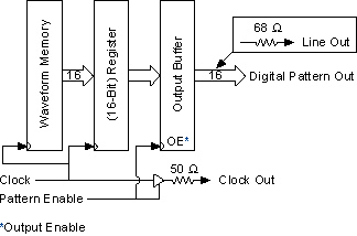
Because the digital pattern data does not go through the digital filter, the data is available directly from the memory. Direct memory access means a fixed delay of 26 Sample clocks between the analog waveform, which lags behind the digital waveform, and the digital patterns exists. Although you can disable the digital filter using the niFgen Configure Digital Filter VI or the niFgen_DisableDigitalFilter function in software, 26 Sample clock delay still exists.
You can enable or disable digital pattern generation by using the niFgen Configure Digital Patterning VI or the niFgen_EnableDigitalPatterning function. All linking and looping capabilities are available for digital pattern generation as well. If you select Function Generation mode, the function generation data appears at the digital I/O connector.
You can use digital pattern generation to test digital devices, such as serial and parallel DACs, and to emulate protocols.
| Note At computer power-up and reset, digital pattern generation is disabled. |
The following figure shows the timing waveforms for digital pattern generation; tclk is the clock time period and tco is the time delay from clock to output on pattern lines, such as PA<0..15>.
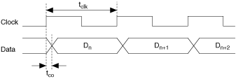
The Sample clock for integral subdivisions of 40 MHz always has a high pulse width of 25 ns. If the tco time is insufficient for the hold time of the device, you can use the falling edge of the Sample clock output (PCLK) to register the digital pattern data.