NI 5402/5406
Phase-Locked Loop Reference Clock
A phase-locked loop (PLL) is a circuit that tunes the Sample clock timebase to phase–lock to an external Reference clock. The frequency stability and accuracy of the Sample clock timebase matches that of the Reference clock when the two phase–lock. Using the PLL on your device enables you to frequency-lock multiple devices in a single chassis, or devices in separate chassis.
 |
Note Refer to the module specifications for information about the phase-locked loop reference frequencies available on your device. |
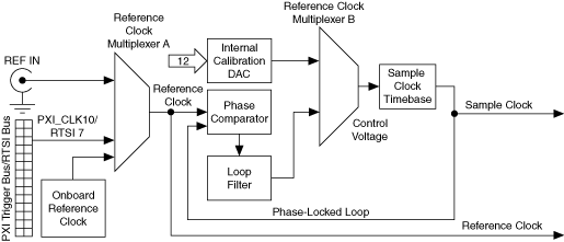
The following figure shows the NI 5402/5406 Reference Clock Source path.

To begin the PLL, the phase comparator compares the selected Reference clock to the 100 MHz clock of the Sample clock timebase. Next, a control voltage proportional to the phase difference between the two clocks is developed and used to tune the Sample clock timebase into alignment with the Reference clock. Finally, the Sample clock timebase output is routed back to the phase comparator, closing the loop.
 |
Note When the Reference Clock Source property or the NIFGEN_ATTR_REFERENCE_CLOCK_SOURCE attribute is set to "None", the internal calibration DAC generates the calibration voltage and the PLL circuit is not used. |
Reference Clock Sources
The NI 5402/5406 is capable of phase–locking its Sample clock timebase to either an external signal on the REF IN front panel connector. PXI devices can also phase–lock to a 10 MHz Reference clock signal provided by the PXI bus (PXI_CLK10), while PCI devices can phase–lock to RTSI line 7 or to the onboard Reference clock.
The following table shows the valid NI-FGEN property or attribute values and combinations to configure the NI 5402/5406 clock settings for an external Reference clock.
| Sample Clock Source | PLL Reference Clock Source |
|---|---|
Internal VXCO(100 MHz) |
"None" (default) |
"PXI_CLK10" (PXI), "RTSI7" (PCI) | |
"RefIn" | |
"OnboardRefClk" (PCI) |
Refer to the module specifications for information about available REF IN signal levels.
Refer to the niFgen Configure Reference Clock VI or the niFgen_ConfigureReferenceClock function for more information about setting up the clock.