NI 5402/5406
Block Diagram
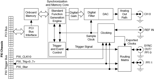
This topic contains information about the NI 5402/5406 top-level block diagram and descriptions of the individual blocks.
;)
 |
Note If it is installed in any slot other than Slot 2 of the PXI chassis, the NI 5402/5406 can receive a signal on the PXI_STAR line and can route a signal on the PXI_STAR line back to Slot 2 of the PXI chassis. |
The following list describes the individual blocks:
- The Onboard Memory stores the frequency list instructions that you load into the device.
- Clocking allows you to phase lock the onboard Sample clock to a Reference clock.
- The Standard Function Generation Engine generates standard functions using direct digital synthesis (DDS) with a 16 k lookup table and 48-bit accumulator using the 100 MHz Sample clock.
- The Standard Function Generation Engine retrieves the frequency list instructions from the Onboard Memory.
- The output from the Standard Function Generation Engine is sent to the DAC after any digital gain is applied.
- For user-defined waveforms, the DAC also contains a selectable Digital Filter, which interpolates and filters the waveform data.
- The waveform data is sent from the DAC to the Analog Output path where the signal data is filtered and amplified.
- The Routing Matrix allows flexible routing of the PXI Trigger lines (RTSI) and the external PFI lines.