NI PXI-5404
Phase-Locked Loop and Module Synchronization
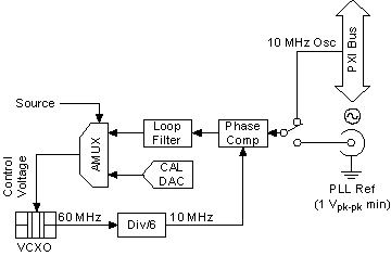
The NI PXI-5404 has an onboard, voltage-controlled crystal oscillator (VCXO) with a tuning range of ±50 ppm. The VCXO generates the main clock of 60 MHz. You can lock the PLL to a Reference clock source from the external REF IN connector, from any of the PXI trigger bus (RTSI) lines or from the 10 MHz backplane clock.
The PLL circuitry divides both the VCXO and the Reference clock down to 1 MHz. A phase comparator then compares the two 1 MHz signals and sends out an error signal. This error signal is filtered and sent to the control pin of the VCXO whose frequency gets adjusted. To achieve phase-locked looping correctly, the external Reference clock must be a multiple of 1 MHz and should have a frequency error of no more than ±50 ppm. The REF IN connector handles frequencies from 3 MHz to 20 MHz and amplitudes from 250 mVpk-pk to 5 Vpk-pk.
The following figure shows the block diagram for the NI 5404 device PLL circuit.
 |
Caution Do not increase the voltage level of the clock signal at the REF IN connector by more than the specified limit, 5 Vpk-pk. |
 |
Note If you lock two or more NI 5404 signal generators to each other using the same Reference clock, they are frequency locked, but the initial phase relationship is indeterminate. You can adjust phase programmatically after the generation is initiated. |