High Voltages
 |
Caution All cables, connectors, and fixtures used in your system must have specifications to handle with an adequate safety margin 1000 V signals for the NI 4071 and 300 V signals for the NI 4065 and NI 4070/4072. |
When switching high-voltage signals, the parasitic capacitance of the cable connecting the NI 4065 and NI 4070/4071/4072 with the switches, as well as the input capacitance of the instrument, needs to be charged to the source voltage. Depending on the voltage present at the DMM input during the measurement on the previous channel, a significant current can flow from the high–voltage source to charge this capacitance.
This current transient does not cause any degradation effect on the NI 4065 and NI 4070/4071/4072, but this action, referred to as hot switching, can reduce the life of the switches. Refer to Handling High DC Voltages for more information about the degradation effect, and refer to the switch documentation for information about extending switch life.
When switching high-voltage signals into a low-voltage range of any DMM (such as applying 300 V on the 10 V range), the input impedance is lower than it is when the proper range is selected. Repetitive operations such as these may shorten switch life. To maximize switch life, always select a measurement range that can handle the maximum voltage expected.
Remember that you might need to increase the settling time of your measurement. Consider the following illustration showing a DMM connected to a 100 V DC source, a thermocouple, and device under test (DUT) through a multiplexing switch.
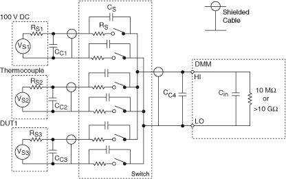
For example, assume you are switching from the 100 V range to the 100 mV range and want to obtain the best sensitivity using the thermocouple. When the switch module advances from the 100 V channel to a thermocouple channel, the input signal conditioning of the DMM (along with the cabling, switching module, and so on) must discharge any stray capacitance from 100 V to 100 µV. If you need a sensitivity of 1 µV from the low–voltage channel, the system must settle from 100 V to 1 µV (10 parts per billion, or eight decades).
When you require resolutions better than 10 ppm, dielectric absorption is a major factor.
Depending upon the source resistance (R), system capacitance (C), and dielectric qualities of the system components, you must allow more settling time in this example. In practice, you may need to allow settling times of 10 ms or more in situations where you are switching high voltages (>30 V).