PCI-CAN
High-Speed Physical Layer
The CAN physical layer circuitry interfaces the CAN protocol controller to the physical bus wires. The PCI-CAN High-Speed physical layer is powered internally (from the card) through a DC-DC converter, and is optically isolated up to 500 VDC(withstand, 2s max) channel-to-bus. This isolation protects the NI CAN hardware and the PC it is installed in from being damaged by high-voltage spikes on the CAN bus.
Transceiver
PCI-CAN High-Speed hardware uses the Philips TJA1041 High-Speed CAN transceiver. The TJA1041 is fully compatible with the ISO 11898 standard and supports baud rates up to 1 Mbps. This device also supports advanced power management through a low-power sleep mode. This feature is provided as the Transceiver Mode attribute of the Frame API and the Interface Transceiver Mode property of the Channel API. For detailed TJA1041 specifications, refer to the Philips TJA1041 data sheet.
Bus Power Requirements
Because the High-Speed physical layer is completely powered internally, there is no need to supply bus power. The V– signal serves as the reference ground for the isolated signals. Refer to PCI and PXI Connector Pinout for information about how to connect signals to a High-Speed CAN interface.
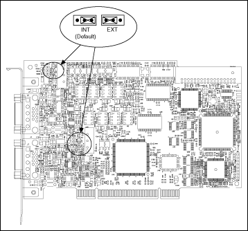
VBAT Jumper
The TJA1041 features a battery voltage input pin, VBAT. This signal can be supplied either internally or externally through the CAN bus V+ signal, as controlled by the VBAT jumper setting. By default, the jumper is set to INT, and VBAT is supplied internally. Some applications may require explicit control of the transceiver VBAT pin; for example, to test the performance of CAN devices on a network where battery power is lost. If external control of VBAT is required, you can configure the PCI-CAN hardware by switching the VBAT jumper from its default INT position to EXT, as shown in the following figure.
With the VBAT jumper set to EXT, you must supply power on the CAN V+ signal. The power supply should be a DC power supply with an output of 8 to 27 V, as specified in the following table. You should take these requirements into account when determining the bus power supply requirements for the system.
| CAN V+ Signal Power Supply | |
|---|---|
| Characteristic | Specification |
| Voltage | 8-27 VDC on V+ connector pin (referenced to V-) |
| Current | 30 μA typical 40 μA maximum |
If you are unsure how to configure VBAT, leave the jumper set to its default value, INT.
Low-Speed/Fault-Tolerant Physical Layer
The PCI-CAN Low-Speed/Fault-Tolerant physical layer is powered internally (from the card) through a DC-DC converter, and is optically isolated up to 500 VDC(withstand, 2s max) channel-to-bus. This isolation protects the NI CAN hardware and the PC it is installed in from being damaged by high-voltage spikes on the CAN bus.
Transceiver
PCI-CAN Low-Speed/Fault-Tolerant hardware uses the Philips TJA1054A Low-Speed/Fault-Tolerant transceiver. The TJA1054A supports baud rates up to 125 kbps. The transceiver can detect and automatically recover from the following CAN bus failures:
- CAN_H wire interrupted
- CAN_L wire interrupted
- CAN_H short-circuited to battery
- CAN_L short-circuited to battery
- CAN_H short-circuited to VCC
- CAN_L short-circuited to VCC
- CAN_H short-circuited to ground
- CAN_L short-circuited to ground
- CAN_H and CAN_L mutually short-circuited
The TJA1054A supports advanced power management through a low-power sleep mode. This feature is provided as the Transceiver Mode attribute of the Frame API and the Interface Transceiver Mode property of the Channel API. For detailed specifications about the TJA1054A, refer to the Philips TJA1054 data sheet.
Bus Power Requirements
Because the Low-Speed/Fault-Tolerant physical layer is completely powered internally, there is no need to supply bus power. The V- signal serves as the reference ground for the isolated signals. Refer to PCI and PXI Connector Pinout for information about how to connect signals to a Low-Speed/Fault-Tolerant CAN interface.
VBAT Jumper
The TJA1054A features a battery voltage input pin, VBAT. This signal can be supplied either internally or externally through the CAN bus V+ signal, as controlled by the VBAT jumper setting. By default, the jumper is set to INT, and VBAT is supplied internally. Some applications may require explicit control of the transceiver VBAT pin; for example, to test the performance of CAN devices on a network where battery power is lost. If external control of VBAT is required, you can configure the PCI-CAN hardware by switching the VBAT jumper from its default INT position to EXT, as shown in the following figure.
Low-Speed/Fault-Tolerant VBAT Jumper Settings
With the VBAT jumper set to EXT, you must supply power on the CAN V+ signal. The power supply should be a DC power supply with an output of 8 to 27 V, as specified in the following table. You should take these requirements into account when determining the bus power supply requirements for the system.
| CAN V+ Signal Power Supply | |
|---|---|
| Characteristic | Specification |
| Voltage | 8-27 VDC on V+ connector pin (referenced to V-) |
| Current | 30 μA typical 125 μA maximum |
If you are unsure how to configure VBAT, leave the jumper set to its default value, INT.
Single Wire Physical Layer
The Single Wire physical layer is powered internally (from the card) through a DC-DC converter. However, the Single Wire CAN transceiver does require bus power. The physical layer is optically isolated up to 500 VDC(withstand, 2s max) channel-to-bus. This isolation protects the NI CAN hardware and the PC it is installed in from being damaged by high-voltage spikes on the CAN bus.
Transceiver
Single Wire hardware uses the Philips AU5790 Single Wire CAN transceiver. The AU5790 supports baud rates up to 33.3 kbps in normal transmission mode and 83.3 kbps in High-Speed transmission mode. The achievable baud rate is primarily a function of the network characteristics (termination and number of nodes on the bus), and assumes bus loading as per SAE J2411. Each Single Wire CAN port has a local bus load resistance of 9.09 kΩ between the CAN_H and RTH pins of the transceiver to provide protection against the loss of ground. The AU5790 also supports advanced power management through low-power sleep and wake-up modes. For detailed AU5790 specifications, refer to the Philips AU5790 data sheet.
Bus Power Requirements
The Single Wire physical layer requires external bus power to provide the signal levels necessary to fully use all AU5790 operating modes. This is because some modes require higher signal levels than the internal DC/DC converter on the PCI-CAN board can provide. You must supply power on the CAN V+ signal. The power supply should be a DC power supply with an output of 8 to 18 V, as specified in the following table. A power supply of 12 VDC is recommended. You should take these requirements into account when determining requirements of the bus power supply for the system.
| CAN V+ Signal Power Supply | |
|---|---|
| Characteristic | Specification |
| Voltage | 8-18 VDC (12 VDC typical) on V+ connector pin (referenced to V-) |
| Current | 40 mA typical 90 mA maximum |
VBAT Jumper
Because the AU5790 requires external bus power, there is no option to power the VBAT signal internally. For this reason, the VBAT jumper is not present on Single Wire hardware, and external bus power must be provided.
XS Software Selectable Physical Layer
PCI-CAN/XS hardware allows you to select each port individually in the physical layer for one of the following transceivers:
- High-Speed
- Low-Speed/Fault-Tolerant
- Single Wire
- External
When an XS port is selected as High-Speed, it behaves exactly as a dedicated High-Speed interface with the TJA1041 transceiver.
When an XS port is selected as Low-Speed/Fault-Tolerant, it behaves exactly as a dedicated Low-Speed/Fault-Tolerant interface with the TJA1054A transceiver.
When an XS port is selected as Single Wire, it behaves exactly as a dedicated Single Wire interface with the AU5790 transceiver.
Note that the bus power requirements and VBAT jumper setting for an XS port depend on the mode selected. Refer to the appropriate High-Speed, Low-Speed/Fault-Tolerant, or Single Wire physical layer section to determine the behavior for the mode selected. For example, the bus power requirements and VBAT jumper operation for an XS port configured for Single Wire mode are identical to those of a dedicated Single Wire node.
When an XS port is selected as external, all onboard transceivers are bypassed, and the CAN controller RX, TX, and mode/status control signals are routed directly to the I/O connector. Refer to PCI and PXI Connector Pinout for information about how to connect signals to an XS CAN interface.
External mode is intended for interfacing custom physical layer circuits to NI CAN hardware. For example, to use a particular CAN transceiver that is not supported natively by the NI CAN hardware, you can use an XS port configured for external mode to connect to the custom-built transceiver circuit and access the bus as usual using NI-CAN software. In addition to the CAN controller RX and TX signals, you also can control two MODE output pins and one STATUS input pin on an external mode port. These MODE and STATUS signals are useful for controlling the operating mode of the custom physical layer and monitoring for any error conditions on the bus. These pins are provided in software as the Transceiver External Outputs (and Inputs) attribute of the Frame API and the Interface Transceiver External Outputs (and Inputs) property of the Channel API.
Because power is not routed through the connector of an XS port, an external transceiver circuit requires bus power to be supplied.
You can change the transceiver type within MAX using the Properties dialog for each port. The transceiver type selected within MAX is used as the default for NI-CAN applications. The initial transceiver configuration in MAX is High-Speed for Port 1 and Low-Speed/Fault-Tolerant for Port 2.
You also can change the transceiver type within the application, which overrides the value in MAX. This feature is provided as the Transceiver Type attribute of the Frame API, and the Interface Transceiver Type property of the Channel API.
RTSI
The RTSI bus gives you the ability to synchronize multiple NI CAN cards with other National Instruments hardware products such as DAQ, IMAQ, and Motion. The RTSI bus consists of a flexible interconnect scheme for sharing timing and triggering signals in a system. For PCI hardware, the RTSI bus interface is a connector at the top of the card, and you can synchronize multiple cards by connecting a RTSI ribbon cable between the cards that need to share timing and triggering signals. The following figure shows the RTSI signal interconnect architecture for NI PCI-CAN hardware.
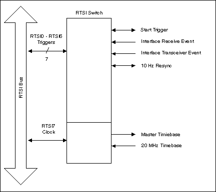
RTSI Signal Interconnect Architecture for NI PCI-CAN Hardware
Refer to the CAN Connect Terminals.vi for a description of the RTSI signals.