Generating LabVIEW FPGA Code (Digital Filter Design Toolkit)
From LabVIEW Digital Filter Design Toolkit
Generating LabVIEW FPGA Code (Digital Filter Design Toolkit)
LabVIEW field-programmable gate array (FPGA) code is a type of code specifically optimized to run on NI Reconfigurable I/O (RIO) devices such as the NI PXI-7831R. LabVIEW FPGA code takes advantage of the specific features, such as the single-cycle Timed Loop (SCTL) and memory items, of the LabVIEW FPGA Module. Therefore, this type of code can run on an FPGA target efficiently. You can use the DFD FXP Code Generator VI to generate LabVIEW FPGA code for filters with the following filter structures:
- FIR structures
- IIR Cascaded Second-Order Sections Form structures
- Lattice MA structures
- Lattice ARMA structures
| Note To generate LabVIEW FPGA code, you must install the LabVIEW FPGA Module and NI-RIO driver software with R Series support. To execute the FPGA code, you also need an FPGA target on which to run the code. |
The LabVIEW Digital Filter Design Toolkit uses LabVIEW projects to manage the resulting LabVIEW FPGA code. The following figure shows an example project file that contains LabVIEW FPGA code.
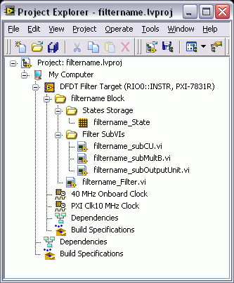
In the previous figure, the filtername.lvproj file, where filtername denotes the name of the fixed-point filter, contains the following folders and VIs in addition to the default items.
- filtername Block—This folder contains all generated VIs and subVIs related to the fixed-point filter from which you generate LabVIEW FPGA code. You can apply the filter to another project by copying and pasting this folder into the target project file.

Note Each filter block contains some FPGA memory components to store the internal states of the fixed-point filter. Multiple filter blocks cannot share the same memory components in one FPGA project. Therefore, if you want to use the filter block multiple times in one FPGA project, you must generate the filter blocks with different filter names from the same fixed-point filter. - States Storage—This folder contains information about the specific resources on an FPGA target, including FIFOs and memory items. These resources store the internal states of the fixed-point filter. You usually do not need to modify the items in this folder.
- Filter SubVIs—This folder contains the generated subVIs. You usually do not need to modify these subVIs.
- filtername_Filter.vi—This VI is the top-level VI of the generated LabVIEW FPGA code. To use the LabVIEW FPGA code, drag and drop this VI to the block diagram of the calling VI.
Refer to the LabVIEW FPGA Code Generation VI in the labview\examples\Digital Filter Design\Fixed-Point Filters\Single-Rate directory for an example that demonstrates how to generate LabVIEW FPGA code from a fixed-point filter.
![]() Open example
Open example
You can generate both one-channel and multichannel LabVIEW FPGA code from a fixed-point filter. Refer to the Lowpass.lvproj file in the labview\examples\Digital Filter Design\Case Studies\Single-Rate Filter\Lowpass directory for an example that demonstrates how to generate one-channel LabVIEW FPGA code from a lowpass, finite impulse response (FIR) filter.
![]() Open example
Open example
Refer to the Notch.lvproj file in the labview\examples\Digital Filter Design\Case Studies\Notch Filter\Notch directory for an example that demonstrates how to generate eight-channel LabVIEW FPGA code from an infinite impulse response (IIR) notch filter.
![]() Open example
Open example
Resolving LabVIEW FPGA Code Compilation Failures
Sometimes the LabVIEW FPGA code might not compile successfully. One potential cause of a compilation failure is that the computation resources on the FPGA target might not meet the requirements of the fixed-point filter. For example, the NI PXI-7831R has 40 built-in 18x18 multipliers. Therefore, you cannot apply filters that require more than 40 built-in multipliers to the NI PXI-7831R. Another potential cause of a compilation failure is that the fixed-point filter is too complicated to implement in an SCTL or that the design clock rate is too high. A more complicated fixed-point filter requires more FPGA hardware resources. The compilation might fail when the FPGA hardware resources are not sufficient. For example, the compilation runs properly when the fixed-point filter uses only 40% of the FPGA hardware resources but the compilation might fail if the fixed-point filter uses about 85% of the FPGA hardware resources. If you encounter compilation failures, try converting the filter structure to one that requires fewer resources or setting the design clock rate to a lower frequency.
The following table lists the number of multiplication units that each filter structure uses. One multiplication unit might require multiple FPGA built-in multipliers, depending on the type of multiplication unit. For example, an I16xI16 multiplication unit requires only one FPGA built-in multiplier, but an I16xI32 multiplication unit requires two FPGA built-in multipliers. This table also lists the estimated execution time in ticks. One tick is one clock cycle, and the clock rate you specify when compiling the FPGA VI determines the length of the clock cycle. Execution time might vary because of the call overhead in loop structures.
| Note Increasing the FPGA target clock rate reduces the amount of code that you can execute in the SCTL because the clock cycle is shorter. |
| Structure | Number of Multiplication Units1 | Estimated Execution Time (ticks)2 | |||||||||||||||
|---|---|---|---|---|---|---|---|---|---|---|---|---|---|---|---|---|---|
| FIR Direct Form | 1B | order+5 | |||||||||||||||
| FIR Direct Form Transposed | 1B | order+5 | |||||||||||||||
| FIR Symmetric (odd order) | 1B | ||||||||||||||||
| FIR Symmetric (even order) | 1B | ||||||||||||||||
| FIR Antisymmetric (odd order) | 1B | ||||||||||||||||
| FIR Antisymmetric (even order) | 1B | ||||||||||||||||
| IIR Cascaded Second-Order Sections Form I | 1A+1B | ||||||||||||||||
| IIR Cascaded Second-Order Sections Form I Transposed | 1A+1B | ||||||||||||||||
| IIR Cascaded Second-Order Sections Form II | 1A+1B | ||||||||||||||||
| IIR Cascaded Second-Order Sections Form II Transposed | 1A+1B | ||||||||||||||||
| Lattice MA (minimum phase) | 1A | order*2+3 | |||||||||||||||
| Lattice MA (maximum phase) | 1A | order*2+4 | |||||||||||||||
| Lattice ARMA (basic sections) | 2A+1B | order+9 | |||||||||||||||
| Lattice ARMA (one multiplier sections) | 1A+1B | order*2+6 | |||||||||||||||
| Lattice ARMA (normalized sections) | 2A+1B | order*2+6 | |||||||||||||||
|
|||||||||||||||||