Conversion Timing for the NI 9205/9206 (FPGA Interface)
The NI 9205 and NI 9206 modules implement a two-element deep pipeline for access to the AI, DI0, and DO0 channels. This pipeline results in maximum sample rate and maximum sample quality. The Trig channel has a parallel data path that bypasses the pipeline.
When using the FPGA I/O Node to sample channels, the pipeline is automatically managed by the FPGA I/O Node, and the channels within the FPGA I/O Node are sampled in numerical order regardless of the order they appear in the node.
If the first two channel requests in the FPGA I/O Node do not match the two channel requests stored in the module pipeline, there will be a delay before the first channel sample occurs. This delay is caused by the FPGA I/O Node automatically updating the module channel sample pipeline, which takes two channel sample cycles.
To minimize the need for the pipeline updates, each FPGA I/O Node leaves the module pipeline primed to repeat itself. If you use only one FPGA I/O Node in a looping structure, only the first iteration of the loop will incur the two-cycle time delay. All subsequent iterations operate with no delay.
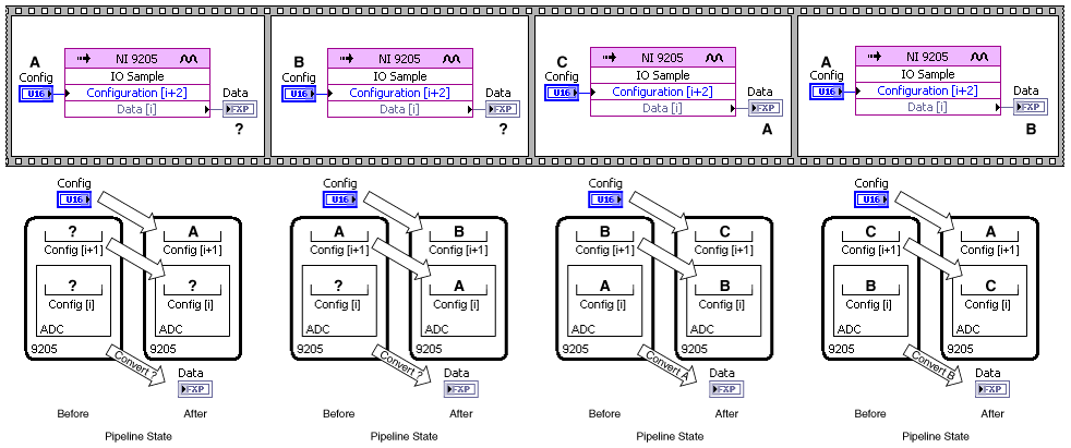
When using the IO Sample method, you must take steps to manage this pipeline in the VIs.
To read one channel, that channel configuration must be requested two cycles before the time it is to be sampled. The U16 configuration value for an AI channel sample contains the channel number, channel input range, and terminal mode. The U16 configuration value also can represent an access to the DIO or DOO channels, which is treated the same as an AI operation.
The following diagram illustrates how the pipeline works within a sequence structure. A typical application would use a loop structure to iterate through a scan list, which is a predefined list of configurations, continuously. The sequence structure and art elements show how data moves into the NI 9205/9206 pipeline and then is converted. Note that the IO Sample method first converts the configuration that is in the ADC, and then shifts the configuration values through the pipeline to prepare for the next time LabVIEW calls the IO Sample method.
The simplest form of pipeline management is to force the pipeline on every set of samples. This assumes that the pipeline is always wrong at the first sample, and sends all IO Sample requests in order. The last two data points need some configuration to be requested, but it does not matter, in this use case, what configuration that is.
A better form of pipeline management emulates the behavior of the FPGA I/O Node. Instead of always assuming that the pipeline is wrong, you choose the last two configuration values based on the first two samples you want to include in the next iteration. This pipeline management system can be accomplished in two parts: initialization and sample iteration.
 |
Tip | National Instruments recommends you use the IO Sample method for the following reasons:
|
The Minimum Time Between Conversions control you can set in the C Series Module Properties dialog box determines the shortest possible time between any two conversions. For channels sampled within the same FPGA I/O Node, the time you set determines the exact time between conversions. For channels sampled within separate FPGA I/O Nodes or for conversions caused by looping on an FPGA I/O Node, the time you set may be less than the actual time between conversions. However, the minimum time you set is never greater than the time between conversions. If the application tries to execute an FPGA I/O Node or IO Sample method faster than the specified minimum time between conversions, the conversion is delayed until the minimum time you set is satisfied.
The default minimum time between conversions for the NI 9205/9206 is 8 µs. The accuracy specifications in the NI 9205 Operating Instructions and Specifications or NI 9206 Operating Instructions and Specifications are based on this default value. If you set the minimum time between conversions to at least 8 µs, the accuracy of the module is not affected. If you set the minimum time between conversions to less than 8 µs, the accuracy of the module degrades if you sample data from multiple channels.
Example
Refer to the Advanced IO example in the labview\examples\CompactRIO\Module Specific\NI 9205\NI 9205 Advanced IO directory for an example of conversion timing on the NI 9205 and NI 9206 C Series Modules.
 Open example