NI RF Signal Generator Hardware Operation
NI RF Signal Generator Hardware Operation
The following figure is the system block diagram of the NI 5650/5651/5652 hardware module. Control signals and data transferred between the circuit blocks are managed by the system control unit. The system control unit contains all the necessary registers for device control from the host computer. Additionally, it contains the temperature monitor and modulation components. Refer to later sections for more information about these and other functions of the system control unit.
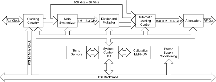
In the upper left hand corner of the diagram is the clocking circuitry. Contained in this circuit are the system clock reference and the direct digital synthesizer (DDS). The system clock is a 200 MHz voltage-controlled crystal oscillator (VCXO) that can be programmed to phase-lock to an external 10 MHz clock signal, present at the REF IN/OUT connector.
The DDS clocked by the 200 MHz reference provides signals of up to 50 MHz, with very fine frequency steps. RF signals below 50 MHz come directly from the DDS. Refer to Using the NI 5650/5651/5652 REF IN/OUT Connector for more information about the onboard reference clock.
Above 50 MHz, signal generation takes place inside the main synthesizer circuit. The synthesizer is phase-locked to the DDS output signal as a reference. This DDS reference signal delivers the necessary fine tuning steps of the synthesizer; the synthesized RF frequency steps are typically 1 Hz or less.
Following the main synthesizer are dividers and multipliers to scale the frequency over the range of 50 MHz to the upper frequency limit of the NI 5650/5651/5652. The lowpass filters implemented allow for an entire octave band, and this impacts the harmonic levels of signals close to the lower end of the octave band. For example, for the NI PXI-5651, a division ratio of 16 results in the octave range of 100 to 200 MHz, and the lowpass filter starts rolloff at 200 MHz. The output of the divided signal contains harmonics: at 100 MHz RF output, the second harmonic is very strong, while at 199 MHz RF output, the second harmonic is suppressed by more than 20 dB. Similarly, during multiplication, the subharmonics are improved at certain frequencies. The worst-case harmonics are specified in the specifications document for your device.
Fine amplitude control is performed by the automatic leveling control (ALC) loop. The ALC has a very broad frequency response, typically from 100 kHz to over 6.6 GHz. The reference for the ALC is set by a temperature-stable voltage DAC. Additional temperature calibration performed during the manufacturing process makes the ALC very stable over the specified operating temperature.
The final block of the system includes the attenuators. These attenuators have a typical range of 100 dB. However, at higher frequencies, reduced isolation limits this range. Thus, the lowest achievable power level increases as the frequency increases.
The calibration data stored in the EEPROM is used by NI-RFSG to correctly set up the hardware for signal generation. Calibration data is used by the instrument driver to compensate for non-ideal components and temperature variation. Refer to Understanding Factory Calibration for more information about calibration data.