 |
Kabylake Intel(R) Firmware Support Package (FSP) Integration Guide
|
3 FSP Integration
3.1 Assumptions Used in this Document
The FSP for the Kabylake platform is built with a preferred base address of 0xFFF40000 and so the reference code provided in the document assumes that the FSP is placed at this base address during the final boot loader build. Users may rebase the FSP binary at a different location with Intel's Binary Configuration Tool (BCT) before integrating to the boot loader.
For other assumptions and conventions, please refer section 8 in the FSP External Architecture Specification version 2.0.
3.2 Boot Flow
Please refer Chapter 7 in the FSP External Architecture Specification version 2.0 for Boot flow chart.
3.3 FSP INFO Header
The FSP has an Information Header that provides critical information that is required by the bootloader to successfully interface with the FSP. The structure of the FSP Information Header is documented in the FSP External Architecture Specification version 2.0 with a HeaderRevision of 3.
3.4 FSP Image ID and Revision
FSP information header contains an Image ID field and an Image Revision field that provide the identification and revision information of the FSP binary. It is important to verify these fields while integrating the FSP as API parameters could change over different FSP IDs and revisions. All the FSP FV segments(FSP-T, FSP-M and FSP-S) must have same FSP Image ID and revision number, using FV segments with different revision numbers in a single FSP image is not valid. The FSP API parameters documented in this integration guide are applicable for the Image ID and Revision specified as below.
The current FSP ImageId string in the FSP information header is $KBLFSP$ and the ImageRevision field is 0x03060000.(3.6.0.0).
3.5 FSP Global Data
FSP uses some amount of TempRam area to store FSP global data which contains some critical data like pointers to FSP information headers and UPD configuration regions, FSP/Bootloader stack pointers required for stack switching etc. HPET Timer register(2) 0xFED00148 is reserved to store address of this global data, and hence boot loader should not use this register for any other purpose. If TempRAM initialization is done by boot loader, then HPET has to be initialized to the base so that access to this register will work fine.
3.6 FSP APIs
This release of the Kabylake FSP supports the all APIs required by the FSP External Architecture Specification version 2.0. The FSP information header contains the address offset for these APIs. Register usage is described in the FSP External Architecture Specification version 2.0. Any usage not described by the specification is described in the individual sections below.
The below sections will highlight any changes that are specific to this FSP release.
3.6.1 TempRamInit API
Please refer Chapter 8.5 in the FSP External Architecture Specification version 2.0 for complete details including the prototype, parameters and return value details for this API.
TempRamInit does basic early initialization primarily setting up temporary RAM using cache. It returns ECX pointing to beginning of temporary memory and EDX pointing to end of temporary memory + 1. The total temporary ram currently available is from 0xFEF0_0000 to 0xFEF4_0000 out of which 0xFEF0_0000(ECX) to 0xFEF3_FF00(EDX) is usable area for both bootloader and FSP binary, remaining 0x100 bytes of space reserved by FSP for TempRamInit if temporary RAM initialization is done by FSP.
TempRamInit** also sets up the code caching of the region passed CodeCacheBase and CodeCacheLength, which are input parameters to TempRamInitApi. if 0 is passed in for CodeCacheBase, the base used will be 4 GB - 1 - length to be code cached instead of starting from CodeCacheBase.
- Note
- : when programming MTRR CodeCacheLength will be reduced, if SKU LLC size is smaller than the requested.
It is a requirement for Firmware to have Firmware Interface Table (FIT), which contains pointers to each microcode update. The microcode update is loaded for all logical processors before reset vector. If more than microcode update for the CPU is present, the microcode update with the latest revision is loaded.
FSPT_UPD.MicrocodeRegionBase** and FSPT_UPD.MicrocodeRegionLength are input parameters to TempRamInit API. If these values are 0, FSP will not attempt to update microcode. If a region is passed, then if a newer microcode update revision is in the region, it will be loaded by the FSP.
MTRRs are programmed to the default values to have the following memory map:
| Memory range | Cache Attribute |
|---|---|
| 0xFEF00000 - 0x00040000 | Write back |
| CodeCacheBase - CodeCacheLength | Write protect |
3.6.2 FspMemoryInit API
Please refer to Chapter 8.6 in the FSP external Architecture Specification version 2.0 for the prototype, parameters and return value details for this API.
The FspmUpdPtr is pointer to FSPM_UPD structure which is described in header file FspmUpd.h.
Boot Loader must pass valid CAR region for FSP stack use through FSPM_UPD.FspmArchUpd.StackBase and FSPM_UPD.FspmArchUpd.StackSize UPDs.
The minimum FSP stack size required for this revision of FSP is 160KB, stack base is 0xFEF17F00 by default.
The base address of HECI device (Bus 0, Device 22, Function 0) is required to be initialized prior to perform FspMemoryInit flow. The default address is programmed to 0xFED1A000.
Calculate memory map determining memory regions TSEG, IED, GTT, BDSM, ME stolen, Uncore PMRR, IOT, MOT, DPR, REMAP, TOLUD, TOUUD. Programming will be done at a different time.
3.6.3 TempRamExit API
Please refer to Chapter 8.7 in the FSP external Architecture Specification version 2.0 for the prototype, parameters and return value details for this API.
If Boot Loader initializes the Temporary RAM (CAR) and skip calling TempRamInit API, it is expected that bootloader must skip calling this API and bootloader will tear down the temporary memory area setup in the cache and bring the cache to normal mode of operation.
This revision of FSP doesn't have any fields/structure to pass as parameter for this API. Pass Null for TempRamExitParamPtr.
At the end of TempRamExit the original code and data caching are disabled. FSP will reconfigure all MTRRs as described in the table below for performance optimization.
| Memory range | Cache Attribute |
|---|---|
| 0x00000000 - 0x0009FFFF | Write back |
| 0x000C0000 - Top of Low Memory | Write back |
| 0xFF800000 - 0xFFFFFFFF (Flash region) | Write protect |
| 0x1000000000 - Top of High Memory | Write back |
If the boot loader wish to reconfigure the MTRRs differently, it can be overridden immediately after this API call.
3.6.4 FspSiliconInit API
Please refer to Chapter 8.8 in the FSP external Architecture Specification version 2.0 for the prototype, parameters and return value details for this API.
The FspsUpdPtr is pointer to FSPS_UPD structure which is described in header file FspsUpd.h.
It is expected that boot loader will program MTRRs for SBSP as needed after TempRamExit but before entering FspSiliconInit. If MTRRs are not programmed properly, the boot performance might be impacted.
The region of 0x5_8000 - 0x5_8FFF is used by FspSilicionInit for starting APs. If this data is important to bootloader, then bootloader needs to preserve it before calling FspSilicionInit.
It is a requirement for bootloader to have Firmware Interface Table (FIT), which contains pointers to each microcode. The microcode is loaded for all cores before reset vector. If more than one microcode update for the CPU is present, the latest revision is loaded.
MicrocodeRegionBase and MicrocodeRegionLength are both input parameters to TempRamInit and UPD for SiliconInit API. UPD has priority and will be searched for a later revision than TempRamInit. If MicrocodeRegionBase and MicrocodeRegionLength values are 0, FSP will not attempt to update the microcode. If a microcode region is passed, and if a later revision of microcode is present in this region, FSP will load it.
FSP initializes PCH audio including selecting HD Audio verb table and initializes Codec.
PCH required initialization is done for the following HECI, USB, HSIO, Integrated Sensor Hub, Display, Sky Cam, Camera, PCI Express, Vt-d, straps (cores, hyper-threading, BIST, ..)
FSP initializes CPU features: XD, VMX, AES, IED, HDC, x(2)Apic, Intel® Processor Trace, Three strike counter, Machine check, Cache pre-fetchers, Core PMRR, Power management.
Initializes HECI, DMI, Internal Graphics. Publish EFI_PEI_GRAPHICS_INFO_HOB during normal boot but this HOB will not be published during S3 resume as FSP will not launch the PEI Graphics PEIM during S3 resume.
Programs SA Bars: MchBar, DmiBar, EpBar, GdxcBar, EDRAM (if supported). Please refer to section 2.8 (MemoryMap) for the corresponding Bar values. GttMmadr (0xDF000000) and GmAdr(0xC0000000) are temporarily programmed and cleared after use in FSP.
On normal boot CPU S3 Resume Data HOB is produced in this phase. This CPU S3 Resume Data HOB is described in section 4.4. Unless UPD SkipMpInit is enabled, on S3 resume, this data (not the entire HOB) must be passed through UPD CpuS3ResumeData, and optionally final S3 boot MTRRs is passed through UPD CpuS3ResumeMtrrData. During S3 resume unless SkipMpInit is enabled, GDT base and length and IDT base and length on APs are programmed to that of the BSP.
3.6.5 NotifyPhase API
Please refer Chapter 8.9 in the FSP External Architecture Specification version 2.0 for the prototype, parameters and return value details for this API.
3.6.5.1 PostPciEnumeration Notification
This phase EnumInitPhaseAfterPciEnumeration is to be called after PCI enumeration but before execution of third party code such as option ROMs. Currently, nothing is done in this phase, but in the future updates, programming may be done in this phase.
3.6.5.2 ReadyToBoot Notification
This phase EnumInitPhaseReadyToBoot is to be called before giving control to boot. It includes some final initialization steps recommended by the BWG, including power management settings, Send ME Message EOP (End of Post).
3.6.5.3 EndOfFirmware Notification
This phase EnumInitEndOfFirmware is to be called before the firmware/preboot environment transfers management of all system resources to the OS or next level execution environment. It includes final locking of chipset registers
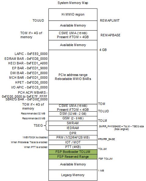
3.7 Memory Map
Below diagram represents the memory map allocated by FSP including the FSP specific regions.
3.8 Porting recommendation
Here listed some notes or recommendation when porting with FSP.
3.8.1 Locking PAM register
FSP 2.0 introduced EndOfFirmware Notify phase callback which is a recommended place for locking PAM registers so FSP by default implemented this way. If it is still too early to lock PAM registers then the PAM locking code inside FSP can be disabled by UPD -> FSP_S_TEST_CONFIG -> SkipPamLock or SA policy -> _SI_PREMEM_POLICY_STRUCT -> SA_MISC_PEI_CONFIG -> SkipPamLock, and platform or wrapper code should do the PAM locking right before booting OS (so do it outside FSP instead) by programming one PCI config space register as below.
This PAM locking step has to been applied in all boot paths including S3 resume.To lock PAM regsiter:
3.8.2 Locking SMRAM register
Since SMRAM locking is recommended to be locked before any 3rd party OpROM execution and highly depending on platform code implementation, the FSP code by default will not lock it. The platform or FSP Wrapper code should lock SMRAM by below programming step before any 3rd partiy OpRom execution (and should be locked in S3 resume right before OS waking vector).
3.8.3 Locking SMI register
Global SMI bit is recommended to be locked before any 3rd party OpROM execution and highly depending on platform code implementation after SMM configuration. FSP by default will not lock it. Boot loader is responsible for locking below regsiters after SMM configuration. Set AcpiBase + 0x30[0] to 1b to enable global SMI. Set PMC PCI offset A0h[4] = 1b to lock SMI.
3.8.4 Verify below settings are correct for your platforms
| Settings | Values |
|---|---|
| PCIEXBAR_BASE_ADDRESS | 0xE0000000 -> PciExBar |
| MCH_BASE_ADDRESS | 0xFED10000 -> MchBar |
| DMI_BASE_ADDRESS | 0xFED18000 -> DmiBar |
| EP_BASE_ADDRESS | 0xFED19000 -> EpBar |
| EDRAM_BASE_ADDRESS | 0xFED80000 -> EdramBar |
| DEFAULT_OPTION_ROM_TEMP_BAR | 0x80000000 -> OpRomScanTempMmioBar |
| DEFAULT_OPTION_ROM_TEMP_MEM_LIMIT | 0xC0000000 -> OpRomScanTempMmioLimit |
- Note
- :
- It is recommended that you do not change these settings as it may require significant changes to the System Agent reference code.
- Those memory regions should be reserved from any memory service functions in platform code so it will not cause any conflict when other modules or drivers allocating memory resource.
- Boot Loader can use different value for PCIEXBAR_BASE_ADDRESS either by modifying the UPD (under FSP-T) or by overriding the PCIEXBAR (B0:D0:F0:R60h) before calling FspMemoryInit Api.
- Boot Loader should avoid using conflicting address when reprogramming PCIEXBAR_BASE_ADDRESS than the recommended one.
- It is recommended that you do not change these settings as it may require significant changes to the System Agent reference code.
3.8.5 FSP_STATUS_RESET_REQUIRED
As per FSP External Architecture Specification version 2.0, Any reset required in the FSP flow will be reported as return status FSP_STATUS_RESET_REQUIREDx by the API.It is the bootloader responsibility to reset the system according to the reset type requested.
Below table specifies the return status returned by FSP API and the requested reset type.
| FSP_STATUS_RESET_REQUIRED Code | Reset Type requested |
|---|---|
| 0x40000001 | Cold Reset |
| 0x40000002 | Warm Reset |
| 0x40000003 | Global Reset - Puts the system to Global reset through Heci or Full Reset through PCH |
| 0x40000004 | Reserved |
| 0x40000005 | Reserved |
| 0x40000006 | Reserved |
| 0x40000007 | Reserved |
| 0x40000008 | Reserved |
Generated on Thu Jun 28 2018 21:44:49 for Kabylake Intel(R) Firmware Support Package (FSP) Integration Guide by
 1.8.10