NI PXI-5412
Block Diagram
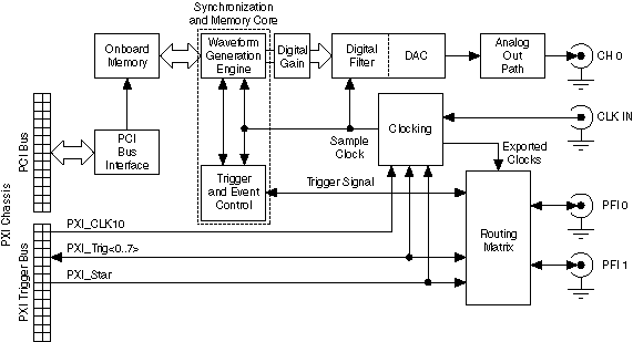
This topic contains information about the NI PXI-5412 top-level block diagram and descriptions of the individual blocks.
;)
 |
Note If it is installed in any slot other than Slot 2 of the PXI chassis, the NI 5412 can receive a signal on the PXI_STAR line and can route a signal on the PXI_STAR line back to Slot 2 of the PXI chassis. |
The following list describes the individual blocks:
- Onboard Memory stores the waveform data and generation instructions that you load into the device.
- Clocking allows you to create your Sample clock and Reference clock.
- The Waveform Generation Engine retrieves the waveform data and instructions from the Onboard Memory using the Sample clock. The Waveform Generation Engine also uses this clock to retrieve triggers from Trigger and Event Control.
- The output from the Waveform Generation Engine is sent to the DAC device after any digital gain is applied.
- The DAC also contains a selectable Digital Filter, which interpolates and filters the waveform data.
- The waveform data is sent from the DAC to the Analog Output path where the waveform data is amplified.
- The Routing Matrix allows flexible routing of the PXI Trigger lines (RTSI) and the external PFI lines.