PWM: Architecture Description
From Modbus RTU XMC47
|
PWM
|
Architecture Description

Figure 1 shows the internal software architecture of the PWM APP. The figure shows the consumed hardware resources, dependent APPs and various signals which are exported out. A PWM APP instance exists in a DAVE™ project with fixed attributes as shown in Figure 1 and uses the CCU peripheral for generating a PWM signal. This in addition requires the consumption of the GLOBAL_CCUx (x =4, 8) and CLOCK APPS for its configuration and functioning. The PWM APP also provides output signals for inter-peripheral connections.
An instantiated APP (after code generation) generates a specific data structure with the GUI configuration. The name of this data structure can be modified by changing the APP instance label (e.g. change label from default PWM_0 to MY_PWM).
Signals:
The following table presents the signals provided by the APP for connection. It also gives the flexibility to configure and extend the connectivity to other APPs.
Table 1: APP I0 signals
| Signal Name | Input/Output | Availability | Description |
| event_period_match | Output | Always | Period match interrupt signal: This can be connected to an INTERRUPT APP to generate the interrupt for each period match event. |
| event_compare_match | Output | Always | Compare match interrupt signal: This can be connected with INTERRUPT APP to generate the interrupt for each compare match event. |
| timer_status | Output | Always | Timer status (ST) signal: This is the slice comparison status value. It can be used as a trigger input to other peripheral modules (e.g. ADC, CCU4, CCU8). |
| pwm_output | Output | Always | Output (OUT) signal:
|
| global_signal | Input | Always | Global signal connection Connected between the kernel and the respective slice. Used to constrain the slice to the kernel provided by GLOBAL_CCUx APP. Connected by default at instantiation. |
CCU in Edge aligned Symmetric Mode of operation.
In this mode of operation we can use the compare registers to generate 1 output. The minimum duty that can be generated is 0% and maximum is 100%. Here the output is initially LOW until compare match happens. The output remains HIGH until the next one match happens.
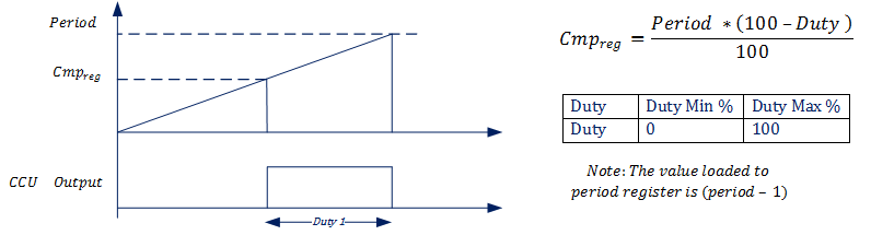
Example:
Let
Note: The value loaded to period register is (period - 1) i.e. 1199.